+48V, Single-Port Network Power Switch
For Power-Over-LAN
4 _______________________________________________________________________________________
ELECTRICAL CHARACTERISTICS (continued)
(V
IN
= 48V, V
DIG
= 3.3V, AGND_S = AGND = DGND = 0V, R
SENSE
= 0.5& ?%, UVLO = open, EN = V
DIG
, R
RCL
= 150& ?%, R
RDT
= 18.2k& ?%, T
A
= -40癈 to +85癈, unless otherwise noted. Typical values are at T
A
= +25癈.) (Note 1)
PARAMETER
SYMBOL
CONDITIONS
MIN
TYP
MAX
UNITS
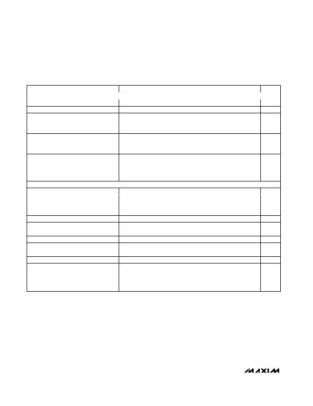
PD DETECTION (See Figure 3, PD Detection Section)
Detection Probe Voltage Phase I
V
PBI
R
PD
= 19k& to 26.5k&
3.6
4
4.4
V
Detection Probe Voltage Phase II
V
PBII
R
PD
= 19k& to 26.5k&
7.2
8
8.8
V
Detection Short-Circuit Current
I
SC_DET
OUT shorted to AGND
0.68
1.50
mA
Valid PD Detected Lower-Limit
Threshold
R
PDL
(Note 9)
15
19
k&
Valid PD Detected Upper-Limit
Threshold
R
PDH
(Note 9)
26.5
33.0
k&
Total Detection Time
t
det
170
196
ms
Reject Capacitance During
Detection
C
PDH
R
PD
= 19k& to 26.5k&
6
礔
Allowable Capacitance During
Detection
C
PDL
R
PD
= 19k& to 26.5k&
0.6
礔
PD CLASSIFICATION (See PD Classification Mode Section)
I
OUT
= 0.5mA to 45mA
15
20
Classification Probe Voltage
V
CLASS
No load
28
V
Classification Short-Circuit
Current
I
SC_CLASS
Shorted to AGND
48
65
mA
Classification Time Duration
t
CLASS
From detection completion
15
21.3
26
ms
Total Detection and Classification
Delay Time
t
TOT
From channel-enabled to power delivered
at the OUT pin
191
230
ms
Class 0 to Class 1 Threshold
I
CLASS_1L
5.5
6.5
7.5
mA
Class 1 to Class 2 Threshold
I
CLASS_1-2
13
14.5
16
mA
Class 2 to Class 3 Threshold
I
CLASS_2-3
21
23
25
mA
Class 3 to Class 4 Threshold
I
CLASS_3-4
31
33
35
mA
Default To Class 0 High-Current
Lower-Limit Threshold
I
CLASS_4-0
43
46.5
mA
Collision Detection Delay Time
(MAX5922A/MAX5922C Only)
t
DCA
DCA = high, R
PD
= 15k&
2.38
2.8
3.22
s
Note 1: All specifications are 100% production tested at T
A
= +25癈, unless otherwise noted. All temperature limits are guaranteed by
design.
Note 2: This is the time from an output overcurrent or short-circuit condition until the output goes into regulated current limit.
Note 3: OUT voltage above which the output current limit is at its full value (see Figure 8).
Note 4: To be consistent with the IEEE 802.3af standard, choose R
SENSE
= 0.5& ?%.
Note 5: This is the time the part stays in current-limit mode during overload condition. After t
OC
elapses (or when the junction temperature
hits +150癈) the part shuts down.
Note 6: See the Typical Operating Characteristics and Figure 6.
Note 7: This is the delay from I
OUT
falling below the zero-current threshold until ZC goes low and the IC shuts down (see the Zero-Current
Detection section).
Note 8: See the Fault Management section.
Note 9: PD is detected by the procedures specified by the IEEE 802.3af standard. A probe voltage V
PBI
(+4V typically) is forced at OUT
and the current I
S1
is measured after t
DET
/2. A second probe voltage V
PBII
(+8V typically) is then forced and I
S2
measured after
t
DET
/ 2 again. The voltage increment is then divided by the difference of the two currents (I
S2
- I
S1
). This is the PD resistance value.
发布紧急采购,3分钟左右您将得到回复。
相关PDF资料
MAX5923EUP+T
IC HOT-SWAP SWITCH +60V 20-TSSOP
MAX5926EEE+
IC HOT-SWAP CONTROLLER 16QSOP-EP
MAX5929BEEG+
IC HOT SWAP CTLR QUAD 24QSOP
MAX5930AEEG+
IC HOT SWAP CTLR PWR SEQ 24QSOP
MAX5932ESA+T
IC HOT-SWAP CONTROLLER 8-SOIC
MAX5933EESA+
IC HOT-SWAP CONTROLLER 8-SOIC
MAX5934EEE+
IC HOT-SWAP CONTROLLER 16-QSOP
MAX5935EAX+
IC CTRLR POWER QUAD 36-SSOP
相关代理商/技术参数
MAX5922AEUI+T
功能描述:热插拔功率分布 48V Single-Port Network Power Switch RoHS:否 制造商:Texas Instruments 产品:Controllers & Switches 电流限制: 电源电压-最大:7 V 电源电压-最小:- 0.3 V 工作温度范围: 功率耗散: 安装风格:SMD/SMT 封装 / 箱体:MSOP-8 封装:Tube
MAX5922AEUI-T
功能描述:热插拔功率分布 RoHS:否 制造商:Texas Instruments 产品:Controllers & Switches 电流限制: 电源电压-最大:7 V 电源电压-最小:- 0.3 V 工作温度范围: 功率耗散: 安装风格:SMD/SMT 封装 / 箱体:MSOP-8 封装:Tube
MAX5922BEUI
功能描述:热插拔功率分布 RoHS:否 制造商:Texas Instruments 产品:Controllers & Switches 电流限制: 电源电压-最大:7 V 电源电压-最小:- 0.3 V 工作温度范围: 功率耗散: 安装风格:SMD/SMT 封装 / 箱体:MSOP-8 封装:Tube
MAX5922BEUI+
功能描述:热插拔功率分布 48V Single-Port Network Power Switch RoHS:否 制造商:Texas Instruments 产品:Controllers & Switches 电流限制: 电源电压-最大:7 V 电源电压-最小:- 0.3 V 工作温度范围: 功率耗散: 安装风格:SMD/SMT 封装 / 箱体:MSOP-8 封装:Tube
MAX5922BEUI+T
功能描述:热插拔功率分布 48V Single-Port Network Power Switch RoHS:否 制造商:Texas Instruments 产品:Controllers & Switches 电流限制: 电源电压-最大:7 V 电源电压-最小:- 0.3 V 工作温度范围: 功率耗散: 安装风格:SMD/SMT 封装 / 箱体:MSOP-8 封装:Tube
MAX5922BEUI-T
功能描述:热插拔功率分布 RoHS:否 制造商:Texas Instruments 产品:Controllers & Switches 电流限制: 电源电压-最大:7 V 电源电压-最小:- 0.3 V 工作温度范围: 功率耗散: 安装风格:SMD/SMT 封装 / 箱体:MSOP-8 封装:Tube
MAX5922CEUI
功能描述:热插拔功率分布 RoHS:否 制造商:Texas Instruments 产品:Controllers & Switches 电流限制: 电源电压-最大:7 V 电源电压-最小:- 0.3 V 工作温度范围: 功率耗散: 安装风格:SMD/SMT 封装 / 箱体:MSOP-8 封装:Tube
MAX5922CEUI+
功能描述:热插拔功率分布 48V Single-Port Network Power Switch RoHS:否 制造商:Texas Instruments 产品:Controllers & Switches 电流限制: 电源电压-最大:7 V 电源电压-最小:- 0.3 V 工作温度范围: 功率耗散: 安装风格:SMD/SMT 封装 / 箱体:MSOP-8 封装:Tube
